Les nouveaux usages d'aujourd'hui seront les business de demain.
Revue de presse sur les tendances et évolutions technologiques utiles.
http://theitwatcher.fr/.
A lire sur: http://spectrum.ieee.org/semiconductors/devices/nanowire-transistors-could-keep-moores-law-alive
Researchers are perfecting ways to produce gate-all-around devices
By Alexander Hellemans / May 2013
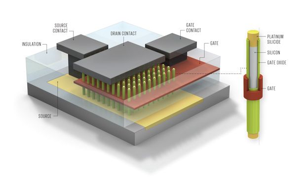
Illustration: Emily CooperGate-All-Around Transistors:
In a new design, the transistor channel is made up of an array of
vertical nanowires. The gate surrounds all the nanowires, which improves
its ability to control the flow of current. Platinum-based source and
drain contacts sit at the top and bottom of the nanowires.
The end of Moore’s Law
has been predicted again and again. And again and again, new
technologies, most recently FinFETs, have dispelled these fears.
Engineers may already have come up with the technology that will fend
off the next set of naysayers: nanowire FETs (field-effect
transistors).
In these nanodevices, current flows through the nanowire
or is pinched off under the control of the voltage on the gate
electrode, which surrounds the nanowire. Hence, nanowire FETs’ other
name: “gate-all-around” transistors. However, because of their small
size, single nanowires can’t carry enough current to make an efficient
transistor.
The solution, recent research shows, is to make a transistor that
consists of a small forest of nanowires that are under the control of
the same gate and so act as a single transistor. For example,
researchers at Hokkaido University and from the Japan Science and
Technology Agency reported last year in Nature
a gate-all-around nanowire transistor consisting of 10 vertical indium
gallium arsenide nanowires grown on a silicon substrate. Although the
device’s electrical properties were good, the gate length—a critical
dimension—was 200 nanometers, much too large for the tiny transistors
needed to power the microprocessors of the 2020s.
Now two researchers working in France, Guilhem Larrieu of the Laboratory for Analysis and Architecture of Systems, in Toulouse, and Xiang‑Lei Han of the Institute for Electronics, Microelectronics, and Nanotechnology, in Lille, report the creation of a nanowire transistor that could be scaled down to do the job.
It consists of an array of 225 doped-silicon nanowires, each 30 nm wide
and 200 nm tall, vertically linking the two platinum contact planes
that form the source and drain of the transistor. Besides their
narrowness, what’s new is the gate: A single 14-nm-thick chromium layer
surrounds each nanowire midway up its length.
That thickness, the gate length, is the key. “The advantage of an
all-around gate allows the creation of shorter gates, without loss of
control on the current through the channel,” explains Larrieu. “We
demonstrated the first vertical nanowire transistor with such a short
gate.” An all-around gate will be a must if gate lengths are to get
smaller than 10 nm, he says. In that scheme, “the size of the gate
depends only on the thickness of the deposited layer; there is no
complicated lithography involved,” he adds.
The nanowires were of an unusual construction. Unlike with most
vertical nanowire transistor prototypes, in which the nano wires are
grown upward from a substrate, the French duo created their nanowires by
starting out with a block of doped silicon and then etching away
material to leave nano pillars. In between the pillars, they deposited
an insulating layer to about half the pillars’ height. Then they
deposited the 14 nm of chromium and filled the remaining space with
another insulating layer. “We tried to make the process completely
compatible with current technology used in electronics. No new machines
will have to be invented,” says Larrieu. The researchers have plans to
try to go below 10-nm gate length, and also to use indium gallium
arsenide nanowires because of the better electron mobility. Kelin Kuhn,
director of advanced device technology at Intel’s Hillsboro, Ore.,
location, agrees that all-around gate structures have some key
advantages. Of all the CMOS-style advanced devices, they’re generally
expected to provide the best gate control for very short channels, she
says. Davide Sacchetto, a
researcher at the École Polytechnique Fédérale de Lausanne, agrees:
“The fabrication of the gate is interesting, and you get a small gate
length.” However, the advantage is lost if the nanowires are too
long—200 nm in this case—and the channel is only a small part of the
total length of the nanowire, he says. “Even a difference of 5 nm would
make a huge difference in the drain current.”
According to Judy Hoyt,
a researcher at the Microsystems Technology Laboratories at MIT,
gate-all-around technology is now under study at a number of university
labs worldwide. But as the nanowire transistors are more complex than
the FinFETs, will this effort allow Moore’s Law to live longer and fit
even more transistors on a chip? “The jury is still out,” says Hoyt. It
depends on what the fabrication process and the structure will be, she
says. “You really have to get the physics right, and that is what all
these efforts are based on.” This article originally appeared in print as "Ring Around the Nanowire."
Aucun commentaire:
Enregistrer un commentaire