Les nouveaux usages d'aujourd'hui seront les business de demain.
Revue de presse sur les tendances et évolutions technologiques utiles.
http://theitwatcher.fr/.
A lire sur: http://spectrum.ieee.org/semiconductors/devices/the-status-of-moores-law-its-complicated/
Node names—the milestones of the chip industry—no longer mean what they used to
By Rachel Courtland
Posted
Illustration: Harry Campbell
One chilly Tuesday evening last December, dozens of
physicists and engineers who dream up tomorrow’s transistors met in San
Francisco to ponder the far future. Would today’s state-of-the-art
switch—a three-dimensional transistor dubbed the FinFET—be able to carry
chips “to the finish,” a distant, possibly unreachable horizon where
transistors are made up of just a handful of atoms? Or would we need a
new technology to get us there?
This may all sound like the tech world’s version of arguing over how
many angels can dance on the head of a pin, but it actually has enormous
real-world implications. The semiconductor industry pulled in revenues of US $300 billion
in 2012. After decades of fulfilling Gordon Moore’s prophesy of
steadily doubling transistor densities (these days every 18 to 24
months), the industry is now delivering integrated circuits with
transistors that are made using what chipmakers call a 20- or
22-nanometer manufacturing process. An IC fabricated with this process,
such as a microprocessor or a dynamic RAM (DRAM) chip, can have billions
of transistors.
Nevertheless, there on the cutting edge, the business is troubled. Each
new generation of ultradense chips demands a new manufacturing process
of mind-boggling industrial and technological complexity. The struggle
has become so pitched that researchers are now often at a loss for words
to describe the metrics of their progress.
At the December meeting, for example, Chenming Hu, the coinventor of the FinFET,
began by mapping out the near future. Soon, he said, we’ll start to see
14-nm and 16-nm chips emerge (the first, which are expected to come
from Intel, are slated to go into production early next year).
Then he added a caveat whose casual tone belied its startling
implications: “Nobody knows anymore what 16 nm means or what 14 nm
means.”
It’s actually become a fairly common refrain among industry experts.
The practice of attaching measurements to chip generations has “been
hijacked by marketers to an enormous extent,” one chip-design expert
told me. “A lot of it’s really smoke and mirrors,” says analyst Dan Hutcheson
of VLSI Research in Santa Clara, Calif. It’s “spin,” he says, that’s
designed to hide widening technological gaps between chip companies.
The nanometer figures that Hu discussed are called nodes, and they are,
for want of a better term, the mile markers of Moore’s Law. Each node
marks a new generation of chip-manufacturing technology. And the
progression of node names over the years reflects the steady progress
that both logic and memory chips have made: The smaller the number, the
smaller the transistors and the more closely they are packed together,
producing chips that are denser and thus less costly on a per-transistor
basis.
But the relationship between node names and chip dimensions is far from
straightforward. Nowadays, a particular node name does not reflect the
size of any particular chip feature, as it once did. And in the past
year, the use of node names has become even more confusing, as chip
foundries prepare to roll out 14-nm and 16-nm chips, custom-made for
smartphone makers and other customers, that will be no denser than the
previous 20-nm generation. That might be just a temporary hiccup, a
one-time-only pause in chip-density improvement. But it’s emblematic of
the perplexing state of the field.
Moore’s Law, when reflected through the steady march of node names,
might seem easy and inexorable. But today a plague of intense
manufacturing and design problems is forcing compromises that are
sometimes sobering. And some analysts suggest that regardless of what we
call the next generation of chips, the transition from old to new no
longer provides nearly the kind of payoff—in cost or performance—that it
used to. “What do you mean by 14 nm?” When I asked An Steegen that
question at an industry conference in July, she smiled and let out a
wry, knowing laugh. “Ah…what’s in a name?” asked Steegen, senior vice
president for process technology development at Imec, the Belgian research center. “Actually, not that much any more.”
It’s a state of affairs that has been nearly two decades in the making.
Once upon a time, the node name told you practically everything you
needed to know about a chip’s underlying technology. If you trained your
microscope on microprocessors made by a handful of different companies
using a 0.35-micrometer process, you’d find that their products were all
remarkably similar.
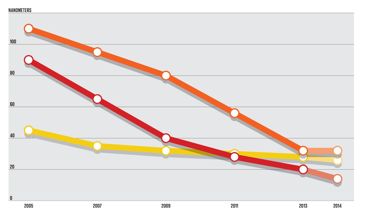
Data Source: GlobalFoundriesWhat’s in a name?
Key chip dimensions, such as the transistor gate length [yellow] and
the metal one half pitch [orange]—half the distance spanned by the width
of a wire and the space to the next one on the dense, first metal layer
of a chip—have decreased but not strictly tracked the node name [red].
These numbers, provided by GlobalFoundries, reflect the company’s plans
to accelerate the introduction of 14 nm chips in 2014, a good year
early.
In the mid-1990s, when such chips were the state of the art, 0.35 µm
was an accurate measure of the finest features that could be drawn on
the chip. This determined dimensions such as the length of the
transistor gate, the electrode responsible for switching the device on
and off. Because gate length is directly linked to switching speed,
you’d have a pretty good sense of the performance boost you’d get by
switching from an older-generation chip to a 0.35-µm processor. The term
“0.35-µm node” actually meant something.
But around that same time, the link between performance and node name
began to break down. In pursuit of ever-higher clock speeds, chipmakers
expanded their tool kit. They continued to use lithography to pattern
circuit components and wires on the chip, as they always had. But they
also began etching away the ends of the transistor gate to make the
devices shorter, and thus faster.
After a while, “there was no one design rule that people could point to
and say, ‘That defines the node name,’” says Mark Bohr, a senior fellow
at Intel. The company’s 0.13-µm chips, which debuted in 2001, had
transistor gates that were actually just 70 nm long. Nevertheless, Intel
called them 0.13-µm chips because they were the next in line. For want
of a better system, the industry more or less stuck to the historical
node-naming convention. Although the trend in the measurements of
transistors was changing, manufacturers continued to pack the devices
closer and closer together, assigning each successive chip generation a
number about 70 percent that of the previous one. (A 30 percent
reduction in both the x and y dimensions corresponds to a 50 percent
reduction in the area occupied by a transistor, and therefore the
potential to double transistor density on the chip.)
The naming trend continued as transistors got even more complex. After
years of aggressive gate trimming, simple transistor scaling reached a
limit in the early 2000s: Making a transistor smaller no longer meant it would be faster or less power hungry. So Intel, followed by others, introduced new technologies to help boost transistor performance. They started with strain engineering,
adding impurities to silicon to alter the crystal, which had the effect
of boosting speed without changing the physical dimensions of the
transistor. They added new insulating and gate materials. And two years ago, they rejiggered the transistor structure to create the more efficient FinFET, with a current-carrying channel that juts out of the plane of the chip.
Through all this, node name numbers continued to drift ever downward,
and the density of transistors continued to double from generation to
generation. But the names no longer match the size of any specific chip
dimension. “The minimum dimensions are getting smaller,” Bohr says. “But
I’m the first to admit that I can’t point to the one dimension that’s
32 nm or 22 nm or 14 nm. Some dimensions are smaller than the stated
node name, and others are larger.”
The switch to FinFETs has made the situation even more complex. Bohr
points out, for example, that Intel’s 22-nm chips, the current state of
the art, have FinFET transistors with gates that are 35 nm long but fins
that are just 8 nm wide.
That is, of course, the view from a chip manufacturer’s side. For his part, Paolo Gargini, the chairman of the International Technology Roadmap for Semiconductors,
says the node is and always has been defined by the proximity of wires
on the first metal layer on the back of the chip, a dimension that was
reflected well in DRAM and, later, flash memory, but not in logic.
Illustrations: Emily CooperTwo Transistors:
Chipmakers are in the process of moving from traditional planar
transistors [left] to ones that pop out of plane [right]. Intel
introduced these 3-D transistors in 2011, and they are now shipping
widely. The leading foundries, such as GlobalFoundries, Samsung, and
Taiwan Semiconductor Manufacturing Co., are in the process of ramping up
production of 20-nanometer planar transistors. They will make the
switch to 3-D with the next generation.
Regardless of definition, numbers in node names have continued
to decline. Along with them, the distance between transistor gates and
that between the closest copper wires on the back of the chip have also
decreased. Both of those features help define how dense a chip can be
and thus how many more you can produce on a single silicon wafer to
drive down costs.
But the difficulty inherent in printing ever-finer features has now
taken its toll. “When we got to around 28 nm, we were actually pushing
the limits of the lithographic tools,” says Subramani Kengeri,
vice president of advanced technology architecture at GlobalFoundries,
the world’s second-biggest chipmaking foundry after Taiwan Semiconductor
Manufacturing Co.
To deal with this, Kengeri and his colleagues were forced to adopt a lithographic technique called double patterning.
It lets technicians pattern smaller features by splitting a single
patterning step into two, relying on a slight offset between the two
steps.
Intel used the technique to form transistors on its 22-nm chips, but it
stuck to single patterning to make the densest metal layer. Pushing the
technique to its limits, the company made wires with a pitch of 80 nm,
which encompasses the width of one wire and the space to the next. By
adopting double patterning, GlobalFoundries and others could push the
pitch down to about 64 nm for their 20-nm chips. But that move came with
a significant trade-off: Double-patterned chips take longer to make,
adding significantly to the cost.
Carrying this technique over from the 20-nm node to 14 nm would mean
that chipmakers would have to double-pattern even more layers of the
chip. So last year, Kengeri and his colleagues announced a chip industry
first: They would put a stop to the shrink. GlobalFoundries’ line of
14-nm chips, which are slated to begin production in 2014, may be the
foundry world’s first FinFET transistors. But the company will build the
new chips with the same wiring density used in its 20-nm chips. “The
first-generation FinFET is basically reusing all of that and plugging a
FinFET into that framework,” Kengeri says. “It’s really a 20-nm FinFET,
in a way.” Nevertheless, the company refers to these as 14-nm chips
because they offer roughly a generation’s-worth jump in performance and
energy efficiency over its 20-nm chips.
Kengeri hopes that by putting a one-generation pause on shrinking chips
and focusing on introducing 3-D transistors, GlobalFoundries will catch up with Intel,
which is already shipping 3-D devices in its 22-nm chips.
GlobalFoundries’ 14-nm chips aren’t any denser than—and therefore cost
just about as much as—the previous generation, but they’re still a big
improvement, Kengeri says. “Our point—and our customers agree—is that as
long as they see that value, they don’t care what the technology is
called or what is inside.”
“It is quite a controversial move,” says William Arnold, chief scientist at ASML,
the world’s largest maker of semiconductor-fabrication equipment. “The
customers of the foundries, the people who are making cellphone parts,
are very skeptical of not being able to get a shrink along with a
performance improvement. They’re pretty vocal about saying that they’re
not happy about that.” The foundries’ latest move aside, chips are still more or less doubling in density from node to node, says Andrew Kahng,
a professor at the University of California, San Diego, and an expert
on high-performance chip design. But for Kahng, the steady progression
of node names masks deeper problems. There is a difference, he says,
between “available density” (how closely you can pack circuits and wires
on a chip) and “realizable density” (what you can actually put into a
competitive commercial product).
The sheer density and power levels on a state-of-the-art chip have
forced designers to compensate by adding error-correction circuitry,
redundancy, read- and write-boosting circuitry for failing static RAM
cells, circuits to track and adapt to performance variations, and
complicated memory hierarchies to handle multicore architectures. The
problem, Kahng says, is that “all of those extra circuits add area.” His
group has been scouring company specs and deconstructing images of
chips for years, and they’ve come to an unsettling conclusion: When you
factor those circuits in, chips are no longer twice as dense from
generation to generation. In fact, Kahng’s analysis suggests, the
density improvement over the past three generations, from 2007 on, has
been closer to 1.6 than 2. This smaller density benefit means costlier
chips, and it also has an impact on performance because signals must be
driven over longer distances. The shortfall is consistent enough, Kahng
says, that it could be considered its own law.
This might be a recoverable loss. So far, Kahng says, the chip industry
has made it a priority to keep up the pace of Moore’s Law, ensuring
that manufacturers can continue to build and release new product
families while using a new process every 18 to 24 months. This means
there hasn’t been time to explore a number of design tricks that could
be used to cut down on power or boost performance. “When you’re on that
kind of schedule, you don’t have time to optimize things,” he says. As
the value of the simple shrink decreases, he says, chipmakers should
then be able to revisit their designs and find chip-improving approaches
they may have missed or else left on the cutting-room floor.
When will the scaling stop? Today’s patterning technology, which relies
on 193-nm laser light, is becoming an ever more costly challenge, and
its natural successor, shorter-wavelength extreme ultraviolet
lithography, has been long delayed.
Kahng says chipmakers may face a more immediate struggle with wiring in
just a few years as they attempt to push chip density down past the
10-nm generation. Each copper wire requires a sheath containing barrier
material to prevent the metal from leaching into surrounding material,
as well as insulation to prevent it from interacting with neighboring
wires. To perform effectively, this sheath must be fairly thick. This
thickness limits how closely wires can be pushed together and forces the
copper wires to shrink instead, dramatically driving up the resistance
and delays and drastically lowering performance. Although researchers
are exploring alternative materials, it’s unclear, Kahng says, whether
they will be ready in time to keep up with Moore’s Law’s steady pace.
Many people in the industry, who have watched showstopper after
showstopper crop up only to be bypassed by a new development, are
reluctant to put a hard date on Moore’s Law’s demise. “Every generation,
there are people who will say we’re coming to the end of the shrink,”
says ASML’s Arnold, and in “every generation various improvements do
come about. I haven’t seen the end of the road map.”
But for those keeping track of the road, those mile markers are starting to get pretty blurry. A version of this article originally appeared in print as “The End of the Shrink.”


Aucun commentaire:
Enregistrer un commentaire