A lire sur: http://www.technologyreview.com/view/522861/worlds-first-photonic-integrated-circuit-for-manipulating-atoms/
 Emerging Technology From the arXiv
December 19, 2013
 Emerging Technology From the arXiv
December 19, 2013
Emerging Technology From the arXiv
December 19, 2013World's First Photonic Integrated Circuit For Manipulating Atoms
The ability to manipulate atoms with photons in an integrated circuit should allow physicists to explore entirely new ways in which matter and light interact.
Electronic integrated circuits are arguably the most significant technology of the 20th century. In enabling, among other things, the computer industry, they have changed the way we work and play to an unprecedented extent.The photonic equivalents of these devices have been equally challenging to develop and are widely used to manipulate and control the signals in optical fibres. But it’s fair to say that they have yet to reach their full potential.
One possibility pregnant with potential is the ability of light to manipulate and influence individual atoms. Physicists regularly use light to trap atoms and ions in the name of science. This has all kinds of important applications from quantum communication to telling the time.
But the devices that do all this are well beyond the reach of anybody unlucky enough not to own a well-equipped optics laboratory.
Photonic integrated circuits could change that. They offer the possibility of of using light to manipulate individual atoms in small self-contained units that are relatively cheap to make and easy to operate.
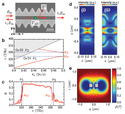
Today, Jeff Kimble at the California Institute of Technology in Pasadena and a few pals say they’ve built the first example of such a device. “We report the development of the first integrated optical circuit with a photonic crystal capable of both localizing and interfacing atoms with guided photons in the device,” they say.
Photonic crystals are useful because their optical properties are determined by the physical geometry, the size of the waveguide and so on. This allows them to be precisely tuned to carry only certain wavelengths of light.
The new device is a photonic crystal made of silicon nitride that acts as a waveguide for laser light.The trick that Kimble and co have perfected is constructing it to carry light tuned to certain atomic transitions in cesium. When a cesium atom absorbs and scatters these wavelengths, the process generates forces that can be used to trap and manipulate the atom.
The photonic crystal is integrated into a system that provides a ready supply of cesium atoms and the result is an integrated circuit capable of manipulating individual cesium atoms.
Kimble and co have put it through its paces and say it works well and offers huge potential. “The integration of nanophotonics and atomic physics has been a long-sought goal that would open new frontiers for optical physics,” they say.
The applications are numerous. This kind of device will be an important high quality building block for quantum computation and communication, since the atoms can store and manipulate information carried by photons.
But the atoms can also act like other kind of optical components, emitting light with almost perfect efficiency or reflecting it like a mirror. And having many atoms interacting with each other and with photons should provide some interesting experimental opportunities for physicists. “The strong interplay between the optical response and large optical forces of many atomic “mirrors” can give rise to interesting opto-mechanical behavior, such as self-organization,” say Kimble and co.
So that’s an interesting proof-of-principle device that could make possible a new generation of nanophotonic experiments. It’s hard to argue at this stage that these kinds of integrated photonic circuits will form the innards of mass-produced devices, as integrated electronic circuits have done. But it’s just as hard to argue that they never will. Only time will tell!

Aucun commentaire:
Enregistrer un commentaire